Loading...

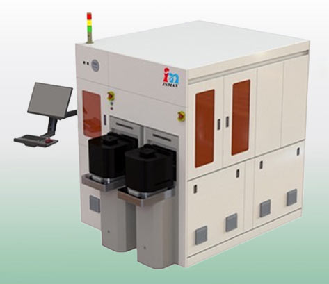
| Features | |
|---|---|
| Resolution | 0.6 µm |
| Process Capability | 2.0~0.6 µm |
| Numerical Aperture (NA) | 0.16 |
| Reduction Ratio | 1:1 |
| Depth of Focus (UDOF) (0.6 µm resist) | ≥3.0 µm |
| Standard Exposure Field | ≥30 x 15 mm |
| Maximum Rectangle Field | 31.8 x 11.4 mm |
| Maximum Square Field | 15.5 x 15.5 mm |
| Projection Lens Distortion (100%) | ≤100 nm |
| Alignment Accuracy (MVS) (100%) | ≤90 nm |
| Wafer Surface Illumination Intensity | >1200 mW/cm² |
| Exposure Spectrum (LED) | 360-370 nm (i-line) |

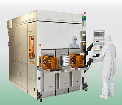
| Features | |
|---|---|
| Resolution | 0.6 µm |
| Process Capability | 2.0~0.6 µm |
| Numerical Aperture (NA) | 0.16 |
| Reduction Ratio | 1:1 |
| Depth of Focus (UDOF) (2 µm resist) | ≥±5 µm |
| Standard Exposure Field | 44 x 26.7 mm |
| Maximum Rectangle Field | 55 x 28 mm |
| - Maximum Square Field | N/A |
| Projection Lens Distortion (100%) | ≤120 nm |
| Alignment Accuracy (MVS) (100%) | ≤200 nm, mean + 3σ |
| Wafer Surface Illumination Intensity | 2800 mW/cm²(ghi) |
| Exposure Spectrum (LED) | 350-450 nm (ghi-line) |